
Overvoltage during IGBT switching
When the IGBT is turned off, the collector current has a high rate of decrease, especially in the case of a short-circuit fault. If no soft-off measures are taken, its critical current decrease rate will reach thousands of amperes per microsecond. The extremely high current decrease rate will induce a high overvoltage on the distributed inductance of the main circuit, causing the current and voltage running trajectories of the IGBT to exceed its safe operating area and be damaged when it is turned off. Therefore, from the perspective of shutdown, it is hoped that the inductance and current decrease rate of the main circuit are as small as possible. However, for the opening of the IGBT, the inductance of the collector circuit is conducive to suppressing the reverse recovery current of the freewheeling diode and the peak current caused by the charging and discharging of the capacitor, which can reduce the opening loss and withstand a higher opening current rise rate. In general, the collector of the IGBT switching circuit does not need a series inductor, and its opening loss can be controlled by improving the gate drive conditions. The buffer protection circuit plays an important role in the safe operation of the IGBT. The following types of buffer protection circuits are commonly used.
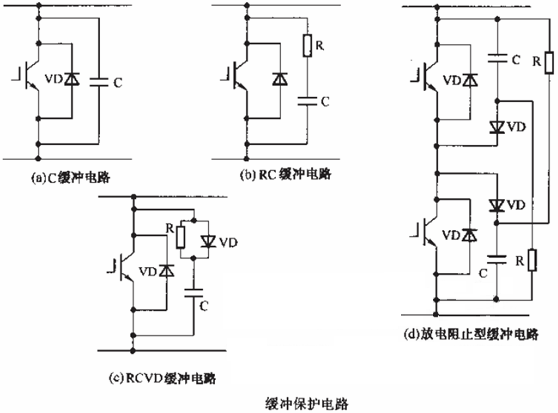
1) C snubber circuit: As shown in the figure below, this circuit uses a film capacitor and is installed close to the
IGBT. Its characteristic is that the circuit is simple. Its disadvantage is that the LC resonant circuit is composed of distributed inductance and snubber capacitor, which is easy to generate voltage oscillation.
2) RC snubber circuit: As shown in Figure (b), its characteristic is that it is suitable for chopper circuits, but when
using large-capacity IGBTs, the resistance of the snubber resistor must be increased, otherwise, the collector
current will be too large when turned on, which will limit the function of the IGBT to a certain extent.
3) RCVD snubber circuit: As shown in Figure (c), compared with the RC snubber circuit, its characteristic is that
a snubber diode is added, thereby increasing the snubber resistor and avoiding the problem of the IGBT function
being blocked when turned on. The loss generated by the snubber resistor in this snubber circuit is
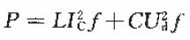
Where: L is the distributed inductance in the main circuit; Ic is the collector current when the IGBT is turned off; f is the switching frequency of the IGBT; C is the snubber capacitor; Ud is the DC voltage value.
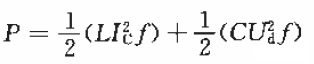
4) Discharge prevention snubber circuit: As shown in Figure (d), compared with the RCVD snubber circuit, its characteristic is that the loss generated is small and it is suitable for high-frequency switching. The loss generated on the buffer resistor in this buffer circuit is
 In circuit design, appropriate buffer protection circuits should be selected according to actual conditions to
suppress the surge voltage when the IGBT is turned off. During assembly, the distributed inductance of the main
circuit and the buffer circuit should be reduced as much as possible, and the shorter and thicker the wiring, the
better.
The buffer absorption circuit of IGBT can be divided into charge-discharge type and discharge prevention type.
There are two types of charge-discharge type: RC absorption and RCVD absorption, as shown in the figure below.
The RC absorption circuit will also cause overshoot voltage because the charging current of capacitor C generates
a voltage drop on resistor R. The RCVD absorption circuit bypasses the charging current on the resistor with a
diode, thereby overcoming the overshoot voltage.
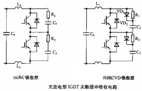
The figure below shows three types of discharge prevention type buffer circuits. In the discharge prevention type buffer circuit, the discharge voltage of the absorption capacitor C1 (C2) is the power supply voltage. Before each shutdown, C1 (C2) only feeds back the overshoot energy of the last shutdown voltage to the power supply, reducing the power consumption of the absorption circuit. Because the capacitor voltage starts to rise from the power supply voltage when the IGBT is turned off, its overvoltage absorption capacity is not as good as that of the RCVD type charge-discharge absorption circuit.

In terms of the ability to absorb overvoltage, the discharge blocking type has a slightly worse absorption effect,
but the energy loss is smaller. The requirements for the buffer absorption circuit are: 1) Minimize the wiring
inductance L of the main circuit. 2) The absorption capacitor should use a low-inductance absorption capacitor,
and its lead should be as short as possible, preferably directly connected to the terminal of the IGBT. 3) The
absorption diode should use a fast turn-on and soft recovery diode to avoid the generation of turn-on
overvoltage and reverse recovery causing a large oscillation overvoltage.