IGBT - DESATURATION PROBLEM
IGBT - Desaturation Problem
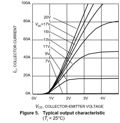
This is the output characteristic curve of a certain product. You can see that the IGBT working area is divided into three parts:
1. Cut-off area: The voltage between CE is less than 0.7V, the PN junction on the back of the IGBT is cut off, and no current flows.
2. Saturation zone: The voltage between CE is greater than 0.7V, current starts to flow, and the voltage between CE rises linearly as the collector current rises. This is the desired working state of IGBT.
3. Amplification area: As the voltage between CE continues to rise, the current further increases. After reaching a certain critical point, the CE voltage increases rapidly, but the collector current does not increase accordingly. At this time we say that the IGBT has exited the saturation zone.
Why Does IGBT Desaturation Occur?
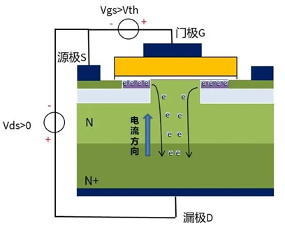
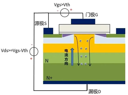
This starts with the planar structure of IGBT. IGBT and MOSFET have similar device structures. The drain D in the MOS is equivalent to the collector C of the IGBT, and the source S of the MOS is equivalent to the emitter E of the IGBT. Both will desaturate. The figure below shows a simplified MOS cross-section diagram to illustrate why desaturation occurs. When a positive voltage VGS greater than the threshold is applied to the gate, a conductive channel will be formed under the gate oxide layer. At this time, if a positive voltage VDS is applied to the drain D, electrons in the source will continue to flow under the action of the electric field. The ground flows from the drain D to the source S, so that a current is formed. At this time, the current increases linearly with the increase of the DS voltage. As the DS voltage increases, the voltage difference between the gate and the silicon surface is very small and the strong inversion of the silicon surface cannot be maintained. The channel pinches off, and the current no longer increases proportionally with the increase in the DS voltage.
So what are the dangers of desaturation in applications?
In practical applications, the desaturation phenomenon generally occurs when the device is short-circuited. At this time, the CE voltage rises to the bus voltage, and the current is generally 4 times the rated current (see the specifications of each device). The power increases abnormally and the junction temperature rises sharply. If the device is not turned off in time, the device may be burned. Most IGBTs have a certain short-circuit withstand capability, generally within 10us. Please refer to each product specification for details.
What To Do If You Encounter Desaturation
1. The simplest method: monitor the current. When the current exceeds a certain threshold, the driver reports an error and turns off the IGBT. This method is essentially overcurrent detection and cannot distinguish overcurrent from desaturation.
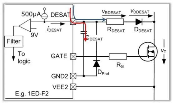
2. Detect the CE voltage of the device. When the IGBT is operating normally, the CE voltage is very low, generally between 1V and 3V. However, the CE voltage will rise rapidly after the IGBT desaturates. The desaturation detection circuit sets a threshold voltage in advance, such as 9V. When the voltage between CE exceeds 9V, the driver chip reports an error and turns off the IGBT. At present, most driver chip manufacturers have launched chips with integrated desaturation detection function, which can be implemented with only simple peripheral circuits. The following is a typical desaturation detection circuit (the power device in the picture is a MOSFET, which can be replaced by an IGBT). The driver chip has a built-in 500uA constant current source. When the device is working normally, the voltage drop is very low, and 500uA current flows through the power device; when the device desaturates, the voltage drop rises sharply, the diode DDESAT is cut off, and the 500uA current can only charge the capacitor CDESAT. When the voltage on CDESAT exceeds 9V, the comparator inside the chip flips and the logic circuit reports an error.
What to pay attention to when desaturating and shutting down
Because the device current is very large in the desaturated state, if the IGBT is turned off without restriction, a large di/dt will be generated, and a high CE voltage will be induced on the parasitic inductance of the loop. If this voltage is high If the rated voltage of the device is exceeded, the IGBT may be damaged. We have two means to control the voltage spike during shutdown
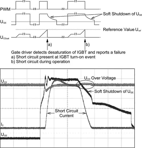
1. Soft turn-off: When the driver detects a short circuit, the soft turn-off function does not directly convert the IGBT gate voltage to 0V or the corresponding negative voltage, but uses a relatively large resistor to pass through it to the gate. The capacitor Cge between them is discharged, thereby reducing the turn-off speed of the IGBT and avoiding overvoltage. Once the gate voltage drops to a certain value (such as 2V), the large resistor is replaced by a small resistor, which ensures that the gate capacitance Cge is quickly and completely discharged.
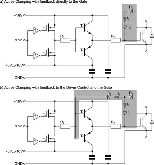
2. Active clamping: The basic principle of active clamping is shown in Figure a. As long as the potential at the collector exceeds a certain voltage threshold UCE, and this voltage is higher than the avalanche voltage of diode VD1, the current I1 flows. Through D1, D2, RG and T2, if the current on RG is greater than the threshold voltage Vth of the IGBT, the IGBT turns on again and the turn-off process slows down, so that the collector voltage is suppressed. This method has higher requirements for the TVS tube and will increase the capacitance between the gate and the collector. Therefore, in practice, a push-pull front stage that feeds the signal back to the gate amplifier is often used, as shown in the figure.