AVALANCHE FAILURE MECHANISM OF MOSFET
1. Latch-Up Effect
In this case, the avalanche event produces a drain current that is larger where the electric field is stronger. The latch-up effect is caused by the parasitic NPN Bipolar Junction Transistor (BJT) in the power MOSFET. If the device is constructed such that the electric field near the parasitic BJT is high, a large amount of current will flow through its base resistor, creating a voltage between the base and emitter. If this voltage reaches a certain threshold, the bipolar transistor turns on and most of the avalanche current flows through it, with potentially damaging effects since there is no way to control the current.
Since the latch-up mechanism is well understood, Infineon has been working hard to mitigate its impact during the development of all OptiMOS™ technologies. Therefore, in many MOSFET technologies, latch-up effects do not occur. However, this is not true for all MOSFET technologies, so it is important to study the data sheet carefully to understand the type of technology used in a particular device and its pros and cons.
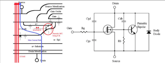
Mosfet Parasitic Bjt Silicon Structure And Equivalent Circuit
1. Thermal failure
Thermal damage occurs when the junction temperature of the MOSFET reaches Tj,destr. Tj,destr is close to the intrinsic temperature of the silicon material, at which the density of hot carriers is equal to the local doping concentration. Therefore, when such temperatures are reached, the MOSFET will no longer behave like a semiconductor device. There is little difference in Tj,destr between OptiMOS™ families, with the value typically approaching 400°C. Given the precautions taken during the technology development of Infineon’s OptiMOS™ family to prevent latch-up effects, thermal damage is responsible for most failures caused by avalanches. Even with latch-up-prone technologies, thermal failure is more likely to occur.
Unfortunately, dealing with thermal damage requires some trade-offs in technology design, as it impacts some of the key drivers of high-performance technology, specifically FOM RDS(on) x A. In fact, while technologies that reduce RDS(on) x A enable smaller chip sizes at a given RDS(on) value, larger die area can mitigate the temperature rise caused by high-energy avalanche events.
2. How To Avoid An Avalanche Event
First, it is necessary to select a device with the correct V(BR)DSS rating for the application. This means that a safety margin of at least 20% should be considered for the maximum steady-state voltage across the drain and source of the device under worst-case operating conditions. In situations where large shutdown transients may occur, higher safety margins will be required for reliable operation
For example, in motor drive inverters it is not uncommon to use MOSFETs with a V(BR)DSS rating of twice the DC bus voltage. However, it would be a mistake to select a device with a higher rating than required, as this will result in higher RDS(on) and potentially higher cost.
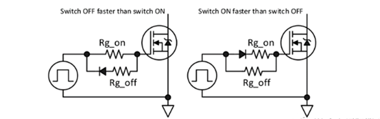
Methods used to reduce turn-off transients include slowing down the MOSFET turn-off by adjusting the gate drive network and adding an RC snubber between the drain and source. Of course, both methods will cause additional switching losses, thereby reducing system efficiency.