SHOWDOWN, THE TRUE FACE OF MOSFET TUBE!
Under normal circumstances, MOS, which is commonly used for high-end driving, needs the gate voltage to be greater than the source voltage when it is turned on. When the MOS tube for high-end driving is turned on, the source voltage is the same as the drain voltage (VCC), so at this time the gate The pole voltage is 4V or 10V greater than VCC.
If you want to get a voltage larger than VCC in the same system, a special boost circuit is needed. Many motor drivers have integrated charge pumps. It should be noted that an appropriate external capacitor should be selected to obtain sufficient short-circuit current. To drive the MOS tube.
The MOS tube is voltage driven. It stands to reason that as long as the gate voltage reaches the turn-on voltage, the DS can be turned on. The gate string can be turned on regardless of the resistance. However, if the switching frequency is required to be higher, the gate to ground or VCC can be regarded as a capacitor.
For a capacitor, the greater the resistance of the string, the longer it takes for the gate to reach the conduction voltage, and the longer the time the MOS is in the semi-conducting state. In the semi-conducting state, the internal resistance is larger, and the heat generation will also increase, which is extremely harmful. MOS is easily damaged, so at high frequencies, the resistance of the gate string must not only be small, but a pre-drive circuit is generally required.
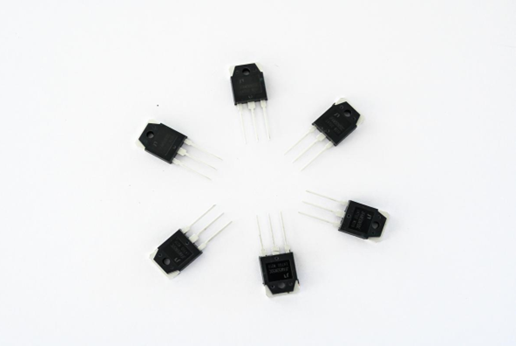
1. Mos Tube Types And Structures
MOSFET is a type of FET that can be made into enhancement mode or depletion mode, P-channel or N-channel, but in practical applications only enhancement-mode N-channel MOS transistors and enhancement-mode P-channel MOS transistors are used. So when NMOS or PMOS are usually mentioned, they refer to these two types.
As for why depletion-type MOS tubes are not used, it is not recommended to get to the bottom of it.
For these two types of enhanced MOS tubes, NMOS is more commonly used because the on-resistance is small and easy to manufacture. Therefore, NMOS is generally used in switching power supply and motor drive applications. In the following introduction, NMOS is mostly used. .
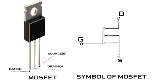
There is a parasitic capacitance between the three pins of the MOS tube. This is not what we need, but is caused by the limitations of the manufacturing process. The existence of parasitic capacitance makes it more troublesome when designing or selecting a drive circuit, but there is no way to avoid it. , which will be introduced in detail later.
Generally, you can see on the schematic diagram of a MOS tube that there is a parasitic diode between the drain and the source. This is called a body diode. This diode is very important when driving inductive loads (such as motors).
By the way, the body diode only exists in a single MOS transistor and is usually not found inside an integrated circuit chip.
1. Mos Tube Conduction Characteristics
Conducting means acting as a switch, which is equivalent to the switch being closed.
Characteristics of NMOS: When Vgs is greater than a certain value, it will turn on. It is suitable for use when the source is grounded (low-end drive), as long as the gate voltage reaches 4V or 10V.
Characteristics of PMOS: It will turn on when Vgs is less than a certain value, which is suitable for situations where the source is connected to VCC (high-end drive).
However, although PMOS can be easily used as a high-end driver, NMOS is usually used in high-end drivers due to large on-resistance, high price, and few replacement types.
2. Mos Switch Tube Loss
Whether it is NMOS or PMOS, there is an on-resistance after it is turned on, so the current will consume energy on this resistor. This part of the energy consumed is called conduction loss.
Choosing a MOS tube with a small on-resistance will reduce the conduction loss. The on-resistance of current low-power MOS tubes is generally around tens of milliohms, and there are also several milliohms.
When MOS is turned on and off, it must not be completed in an instant. The voltage at both ends of the MOS has a declining process, and the current flowing through it has a rising process. During this period, the loss of the MOS tube is voltage and current. The product of is called switching loss.
Usually switching losses are much larger than conduction losses, and the faster the switching frequency, the greater the losses.
The product of the voltage and current at the moment of conduction is very large, and the loss caused is also very large. Shortening the switching time can reduce the loss during each conduction; reducing the switching frequency can reduce the number of switches per unit time. Both methods can reduce switching losses.