
Switching Characteristics Of IGBT Power Modules
The switching characteristics of the IGBT power module are determined by its internal structure, internal parasitic capacitance and internal and external resistance. In an ideal state, we only need a zero-power voltage signal to be applied to the MOS base to activate the switch. But in practice, the charge stored in the capacitor inside the component must be released, so a driving power signal with the same switching frequency is required. In addition, the commutation process is also affected by parasitic inductance. Parasitic inductance exists in the port loop of the module and inside the module, as well as in the connection lines connecting the transistor chips.
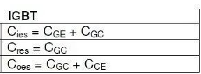
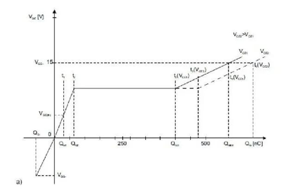
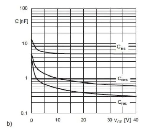
However, these parameters can only be used to a limited extent to calculate the switching characteristics of the IGBT. For example, when the transistor is turned on (VCE < VGE), the input and feedback capacitances increase significantly. Therefore, the gate charge curve is given in the data file, which can be used to approximate the switching time and gate demand.
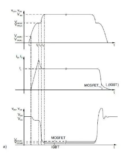
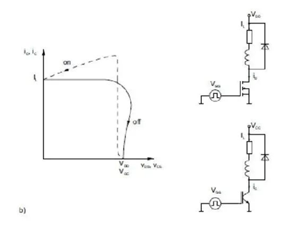
The switching characteristics of an IGBT can be viewed as a hard turn-on and turn-off of only an inductive resistive load. In other words, the load time constant L/R is much larger than the switching period 1/f. The figure depicts the relationship between collector current and collector-emitter voltage and gate control voltage VGE. The figure depicts the mo
vement of the operating point during hard turn-on and turn-off, ic = f(vCE). Because there is only a small difference between power MOSFET and IGBT in this regard, the figure is an explanation of these two components.
The characteristic of hard switching is that the current and voltage of the transistor increase within a short period of time when it is turned on or off, because in the load circuit, the freewheeling diode prevents the sudden change in current caused by the inductance.
When the transistor is turned on, the freewheeling diode can only start to withstand the cut-off voltage (turn off) after the load current has completely commutated into the transistor. Therefore, the collector current must first reach the magnitude of the load current before the collector-emitter voltage drops to the on-state voltage drop value.
When the transistor is turned off, the freewheeling diode only begins to take up the load current (turns on) when its polarity is positive. The occurrence of this condition requires that the collector-emitter voltage first reaches the level of the commutation voltage.

The working point can be kept close to the coordinate axis through a passive buffer network (rarely used nowadays). Switching losses are transferred from the transistor to the snubber circuit, and most of the overall efficiency is reduced. In addition to being limited by current and voltage and switching time, the operating point movement of a transistor is also affected by various other (non-ideal) factors. Therefore, the safe operating area (SOA) applicable to different operating states is given in the data file.
In addition to the impact of the non-ideal characteristics of transistors and diodes, some passive components in the current loop will also have a great impact on power consumption and the movement of the operating point.
As shown in the figure, within tens of nanoseconds after the IGBT is turned on, the collector-emitter voltage will quickly drop to a certain value, which corresponds to the voltage drop in the n-region. Finally the n-region is filled with positive carriers from the p collector. After hundreds of nanoseconds to several microseconds, the dynamic saturation voltage VCE(sat)dyn of IGBT drops to the on-state voltage drop value VCE(sat).
Turn on: 0 to t1 time period (transistor off state)
As the gate voltage turns on, the gate current iG begins to flow. Before reaching the charge quantity QG1, the current iG charges the gate capacitor CGE, and the gate-emitter voltage VGE rises according to a time constant. This time constant is determined by the input capacitance of the IGBT and the resistance of the gate control loop. Because the voltage VGE is less than the threshold voltage VGE(th), there is no collector current during this period.
Turn on: time period from t1 to t2 (collector current rises)
After reaching the threshold voltage VGE(th) (t1), the collector current begins to rise. Similarly, the voltage VGE of the IGBT also rises, because in the active operating area, its relationship with the current and the current rise rate is IC = gfs · VGE . This state lasts until time t2, VGE1 = IC/gfs (time t2). Because the freewheeling diode is not turned off until time t2, VCE will not drop to the rated value before time t2. The amount of electricity stored in the base at time t2 is the amount of electricity QG2. Most of the losses generated by the IGBT occur during this time period, because when the current iC is less than the load current IL, a part of the current must flow through the freewheeling diode, and the collector-emitter voltage vCE at this time has not yet reached the driving voltage. VCC conditions, down to rated value. The figure shows the voltage VCC and VCE deviation. This deviation is mainly caused by the voltage difference on the IGBT and the parasitic inductance in the commutation circuit.
Turn on: t2 to t3 time period (the transistor turns on in the active area, flat area)
As the freewheeling diode turns off, the voltage VCE begins to decrease. By time t3, it is close to the on-state voltage drop VCE(sat). During the period from t2 to t3, the collector current still maintains a transfer rate relationship with the gate control voltage, so the voltage vGE remains almost at a fixed value. During the decrease of voltage vCE, the base current charges the Miller capacitor CCG, and the charging amount is (QG3-QG2). The amount of charge on the base at time t3 is QG3. When the entire load current IL flows through the IGBT after commutation, the freewheeling diode enters the cut-off state. Because of the delay time of the freewheeling diode, when the freewheeling diode enters cutoff, the collector current iC of the IGBT will continue to rise, causing the reverse current IRRM of the diode to exceed the current IL. This causes the amount of cut-off delay charge Qrr in the diode to decrease.
Opening: t3 to t4 time period (saturation zone)
The IGBT is fully turned on at time t3, and its operating point passes through the active zone and begins to enter the saturation zone. The voltage VGE is no longer related to the current IC via the transfer rate gfs. At this time, the increased charge on the gate (QGtot -QG3) causes the gate voltage to further rise until it reaches VGG. Although the collector-emitter voltage VCE rises rapidly, it has not yet reached its stable conduction value VCEsat. It generally takes hundreds of nanoseconds or microseconds to adjust according to the size of the voltage VGG and current IC, together with the carriers in the n-drift region. This time to reach dynamic saturation VCE(sat)dyn = f(t) is the time necessary for (bipolar) overflow carriers (conduction ions) to pass through the IGBT n-drift region.
Turn Off
We can understand turn-off as the reverse workflow of turn-on. The charge QGtot on the base must be released by controlling the current. First the internal capacitor releases charges, which are removed in the flow area. Therefore, in this region, the neutral interference will be eliminated quickly and the collector current will drop quickly in the beginning. When the emitter current is turned off in the n region, there are still a large number of p carriers injected by the IGBT collector in the n drift region. They must be removed through recombination or back-injection. This creates a tail current at the collector. This tail current coincides with the collector-emitter voltage for a few microseconds, which determines the shape and length of the power loss of the IGBT as a hard switch. The figure shows that the voltage vCE overshoots and exceeds the voltage VCC after the turn-off. The main reason for this is the parasitic inductance in the commutation circuit and the increased current conversion rate dic/dt of the IGBT when it is turned off. The more a transistor-based switch deviates from an ideal hard switch (such as an inductive element in a commutation circuit), the more blurred the steps in the base-emitter voltage waveform become. The hard switching characteristics of freewheeling diodes are very complex.