What is desaturation of IGBT? Under what circumstances will the IGBT enter the desaturation state?
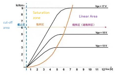
The figure below is a typical output characteristic curve of IGBT products. The horizontal axis is the voltage across C and E, and the vertical axis is the normalized collector current. You can see that the IGBT working status is divided into three parts:
【1.: cut-off area】
The voltage between CE is less than a threshold voltage, that is, the turn-on voltage of the PN junction on the back, the PN junction on the back of the IGBT is cut off, and no current flows.
【2.: Saturation zone 】
After the voltage between CE is greater than the threshold voltage, the current starts to flow, and the voltage between CE increases linearly with the rise of the collector current. This region is called the saturation region. Because the IGBT saturation voltage is low, we hope that the IGBT works in the saturation region.
【3.: Linear Area】
As the voltage between CE continues to rise, the current increases further. After reaching a certain critical point, the CE voltage increases rapidly, but the collector current does not increase accordingly. At this time, we say that the IGBT has exited the saturation region. In this interval, the IGBT loss increases and the heat is severe, which is a working state that needs to be avoided.
Why does IGBT desaturation occur?
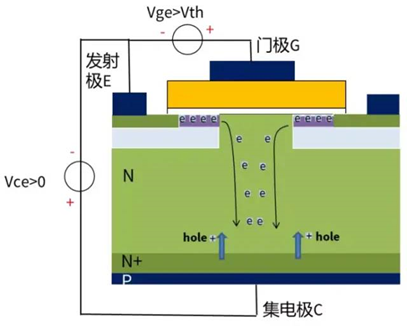
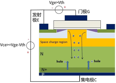
This starts with the planar structure of the IGBT. IGBT and MOSFET have a similar device structure. The drain D in the MOS is equivalent to the collector C of the IGBT, and the source S of the MOS is equivalent to the emitter E of the IGBT. Both of them will experience desaturation. The figure below is a simplified planar IGBT cross-section to illustrate the cause of desaturation. The gate applies a positive voltage VGE greater than the threshold. Then a strong inversion layer appears under the gate oxide layer, forming a conductive channel. At this time, if a positive voltage VCE is applied to the collector C, the electrons in the emitter will continuously flow from the emitter E to the collector C under the action of the electric field, and the holes in the collector will flow from the collector C Flow to the emitter E, so that the current is formed. At this time, the current increases linearly with the increase of CE voltage, and the device works in the saturation region. When the CE voltage is further increased, the potential at the end of the MOS channel increases with VCE, so that the voltage difference between the gate and the silicon surface is very small, and the strong inversion of the silicon surface cannot be maintained. At this time, the channel appears pinch-off, The current no longer increases proportionally with the CE voltage. We say that the device exits the saturation region.