Detailed Explanation Of IGBT Module Parameters - Overall Module Parameters
This section describes the electrical characteristic parameters related to the mechanical structure of the IGBT module, including insulation withstand voltage, main terminal resistance, stray inductance, and DC voltage capability.
Insulation withstand voltage
In order to evaluate the rated insulation voltage value of the IGBT module, connect all terminals together to the high-voltage side of the high-voltage source, and the substrate to the low-voltage side of the test instrument. The high-impedance high-voltage source must provide the required insulation test voltage Viso, gradually increase the test voltage to the specified value, which can be determined by the following formula and maintain the specified time t, and then reduce the voltage to 0. For IGBT modules with internal NTC, the insulation requirements can be verified by connecting high voltage between the grounded NTC and all other control and main terminals connected together.

The appropriate insulation voltage depends on the rated collector-emitter voltage of the IGBT. For 1700V IGBT modules, most applications require an insulation withstand voltage requirement of 2.5KV. But for traction applications, the same 1700 blocking voltage IGBT module requires 4KV insulation withstand voltage capability. Therefore, whe
Main terminal resistance
The resistance of the main terminal of the IGBT module will further cause voltage drop and loss. The specified resistance value of a single switch power terminal is as shown below. This value refers to the resistance value of the connection between the power terminal and the chip. The losses generated at the main terminals are added directly to the module housing.
n selecting IGBT modules, it is very important to pay attention to the application scenarios. Because the insulation test means that the module is subjected to extreme stress, if the customer needs to repeat the test, it is recommended to derate the value by 85% of the original value.

The high-voltage module also uses standard IEC1287 for partial discharge testing to ensure long-term working reliability.

The insulation withstand voltage test shown in the figure above should be performed before and after the reliability test of the IGBT module, and can be used as a partial failure criterion under this stress test.
The insulation of the internal NTC only meets a functional isolation requirement. When the gate drive circuit fails, the bonding wire may change position due to the failure event, and the moving bonding wire or the plasma generated by the arc discharge during the failure process may come into contact with the NTC. Therefore, if there are higher requirements for insulation capacity, additional external insulation partitions need to be added.
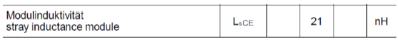
Stray inductance Lδ
Stray inductance can cause surge voltages during switching and is a major source of EMI. At the same time, the parasitic capacitance of the components is combined to form a resonant circuit, causing the voltage and current to oscillate at the switching instant. The instantaneous overvoltage caused by stray inductance can be calculated by the following formula. Therefore, in order to reduce the overvoltage at the moment of turn-off, the stray inductance should be designed to be minimum.
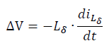
The value of stray inductance inside the IGBT module is shown in the figure below, which depends on the topology of the IGBT.
Main terminal resistance
The resistance of the main terminal of the IGBT module will further cause voltage drop and loss. The specified resistance value of a single switch power terminal is as shown below. This value refers to the resistance value of the connection between the power terminal and the chip. The losses generated at the main terminals are added directly to the module housing.
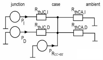
According to the equivalent circuit of the module terminal resistance in the figure below
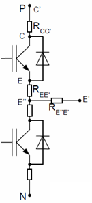
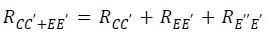
The resistance of the main terminal of the entire module can be obtained as:
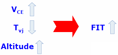
DC stability (VCED)

For high-voltage modules, the impact of cosmic rays will be more severe, and a DC voltage value that will produce a negligible failure rate of 100fit is specified, as shown in the figure above. The DC stable voltage is measured at room temperature and sea level. It is not recommended to set the DC voltage to exceed VCED.