
IGBT module peak voltage absorption circuit
When the IGBT is turned off, a surge voltage will occur between the collector and the emitter due to the energy stored in the inductor. The snubber circuit suppresses overvoltage applied to the IGBT and increases turn-off losses. This is because the snubber capacitor can share part of the energy during shutdown. Be sure to handle the energy absorbed by the capacitor properly.
RCD buffer circuit:
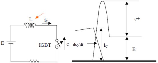
Energy stored when the switch is turned off: 1/2・LiC e+=L・diC/dt
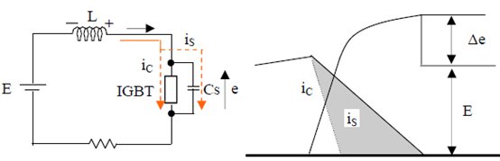
This is true if Cs can completely absorb the energy of L 1/2・LiC2=1/2・Cs・Δe2, so Δe= i0×√L/Cs
Losses of RCD buffer circuit:
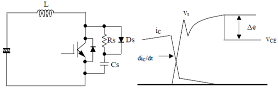
It is more effective to install the snubber circuit on each IGBT than between the DC bus and ground. However, there is a problem of large loss on Rs. The loss on Rs is the product of LiC2 and the switching frequency, which is 20W when L is 0.2μH, iC is 100A, and the switching frequency is 10kHz. At this time, in the three-phase bridge circuit, the loss of the buffer circuit alone is 120W. Losses can be reduced by lowering the frequency or regenerating energy into the power supply. In order to reduce Δe, it is particularly important to first reduce L (the distributed inductance of the main circuit). Cs becomes smaller as the inductance becomes smaller. Vs is the sum of (wiring inductance) ×-dic/dt, the forward recovery voltage of Ds, and (distributed inductance of Cs) ×-dic/dt.
The following points can make the snubber circuit more efficient. ● Drive IGBT with lower -dic/dt as the driving condition. (Reduce the turn-off speed of IGBT) ● Reduce the inductance of the main circuit wiring. To do this, try to place the power supply (electrolytic) capacitor as close as possible to the IGBT module, use copper plate wiring, implement a layered layout, etc. ● The buffer circuit should also be placed near the module, and components with good frequency characteristics such as film capacitors should be used for Cs. ● Ds uses ultra-fast diodes with small forward voltage drop and soft reverse recovery.
Actual buffer circuit:
Example of buffer circuit for each phase
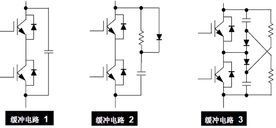
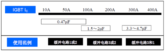
Indicators of snubber capacitor capacity: Snubber circuit 1 on the previous page omits the damping resistor and the power supply wire is easily disturbed by vibration noise, so it is suitable for applications with smaller capacity. When snubber circuits 1 to 3 are classified according to their uses, the standards for the snubber capacitor capacity of each phase are as follows. The capacity of the snubber circuit for each IGBT is 1/2 of this value.
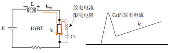
When applied to large power applications, if layered copper wiring is not used to reduce wiring inductance, it may be impossible to avoid component damage in the buffer circuit or malfunction caused by noise interference. Discharge prevention type snubber circuit (buffer circuit 3):
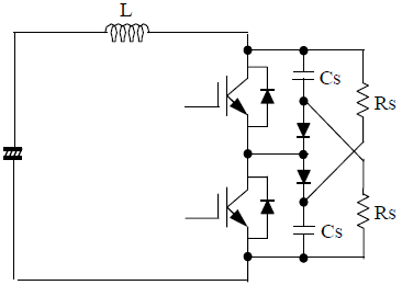
If Cs can absorb all the energy of L 1/2·L·iC2=1/2·Cs·Δe2 Therefore Cs=L×(iC/Δe)2 The charge of Cs needs to be discharged until the next turn-off, for this ( The time constant of Cs×Rs) is valid. In order to discharge 90%Rs≦1/(2.3・Cs・f) f: switching frequency then the minimum value of Rs can be determined. However, if Rs is too small, it will cause harmful oscillations during turn-on, so it is better to use a slightly higher value. The loss P(Rs) on Rs has nothing to do with the value of Rs, and is P(Rs)=1/2・L・iC2