
Analysis of IGBT switching process and driving considerations
The circuit of IGBT under diode clamped inductive load conditions is shown in Figure 1. This circuit is a commonly used IGBT circuit and can be used as a test circuit for IGBT switching characteristics to evaluate the on and off behavior of IGBT. Figure 2 shows the actual IGBT switch waveform obtained by comprehensively considering the recovery characteristics of diodes and stray inductance (Ls), which can be used as a reference for designing IGBT drive circuits. Firstly, we set the IGBT to operate under continuous steady-state current conditions, flowing through an inductive load and then through an ideal freewheeling diode parallel to the inductive load.

Picture1. Diode-Clamped inductive load

Picture 2. IGBT Switching Waveform
The conduction waveform of IGBT is very similar to that of MOSFET. In addition to the trailing current, the turn off characteristics of IGBT are also similar to those of MOSFET. The following time zones will explain the operating principle of IGBT one by one.
a. Conduction process
T0 time period:
During the t0 time period, the gate current iG charges the input parasitic capacitors Cge and Cgc, and VGE rises to the threshold VGE (th). VGE is considered to have a linear increase, but in reality, it is an exponential curve with a time constant of RG (Cge+Cgc). During this time, VCE and iC remain unchanged. The conduction delay time is defined as the time from the gate voltage rising to 10% of VGG+to the collector current iC rising to 10% of Io. Therefore, most of the conduction delay time is in the t0 time period.
Time period t1:
When VGE exceeds VGE (th), a channel is formed in the base region below the gate oxide layer, and current begins to conduct. During this time, IGBT is in the linear region, and iC increases with VGE. The increase in iC is related to the increase in VGE, ultimately reaching the full load current Io. During time periods t1 and t2, the value of VCE slightly decreases relative to Vd, due to the voltage VLS=LS * diC/dt caused by the stray inductance in the circuit, which is generated at both ends of LS and opposite to the direction of Vd. When iC increases, the value of VCE decreases depending on diC/dt and LS, and the shape changes with the form of iC.
Time periods t2 and t3:
The diode current iD starts to decrease during the t1 time period, but it cannot immediately drop to 0A because there is a reverse recovery process, and the current will flow in the opposite direction. Reverse recovery current is superimposed on iC, making the iC form the same for time periods t2 and t3. At this moment, the reverse voltage at both ends of the diode increases, and the voltage drop VCE at both ends of the IGBT decreases. Because the value of Cge is small when VCE is large, VCE rapidly decreases, resulting in a larger dVCE/dt at this time. Within t3 time, Cgc absorbs and discharges the gate driving current, while Cge discharges. At the end of the t3 time period, the reverse recovery process of the diode ends.
Time period t4:
During this period, iG charges Cgc, while VGE remains at VGE, IO, and iC remains at full load current Io, while VCE decreases at a rate of (VGG-VGE, Io)/(RGCgc). The VCE drops significantly and there is a trailing voltage, which is because the value of Cgc is larger at low VCE
Time period t5:
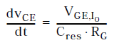
During this period, VGE increased again with the time constant RG (Cge+Cgc, miller) until VGG+, Cgc, miller is the Miller capacitance, and due to the Miller effect, it increases with the decrease of VCE. Within t5 time, VCE slowly decreases to the collector emitter saturation voltage and fully enters a saturation state. This is because the speed of IGBT transistors passing through the linear region is slower than that of MOSFETs, as well as the influence of Miller capacitors Cgc and Miller.
The conduction waveform of IGBT is very similar to that of MOSFET. In addition to the trailing current, the turn off characteristics of IGBT are also similar to those of MOSFET. The following time zones will explain the operating principle of IGBT one by one.
a. Conduction process
T0 time period:
During the t0 time period, the gate current iG charges the input parasitic capacitors Cge and Cgc, and VGE rises to the threshold VGE (th). VGE is considered to have a linear increase, but in reality, it is an exponential curve with a time constant of RG (Cge+Cgc). During this time, VCE and iC remain unchanged. The conduction delay time is defined as the time from the gate voltage rising to 10% of VGG+to the collector current iC rising to 10% of Io. Therefore, most of the conduction delay time is in the t0 time period.
Time period t1:
When VGE exceeds VGE (th), a channel is formed in the base region below the gate oxide layer, and current begins to conduct. During this time, IGBT is in the linear region, and iC increases with VGE. The increase in iC is related to the increase in VGE, ultimately reaching the full load current Io. During time periods t1 and t2, the value of VCE slightly decreases relative to Vd, due to the voltage VLS=LS * diC/dt caused by the stray inductance in the circuit, which is generated at both ends of LS and opposite to the direction of Vd. When iC increases, the value of VCE decreases depending on diC/dt and LS, and the shape changes with the form of iC.
Time periods t2 and t3:
The diode current iD starts to decrease during the t1 time period, but it cannot immediately drop to 0A because there is a reverse recovery process, and the current will flow in the opposite direction. Reverse recovery current is superimposed on iC, making the iC form the same for time periods t2 and t3. At this moment, the reverse voltage at both ends of the diode increases, and the voltage drop VCE at both ends of the IGBT decreases. Because the value of Cge is small when VCE is large, VCE rapidly decreases, resulting in a larger dVCE/dt at this time. Within t3 time, Cgc absorbs and discharges the gate driving current, while Cge discharges. At the end of the t3 time period, the reverse recovery process of the diode ends.
Time period t4:
During this period, iG charges Cgc, while VGE remains at VGE, IO, and iC remains at full load current Io, while VCE decreases at a rate of (VGG-VGE, Io)/(RGCgc). The VCE drops significantly and there is a trailing voltage, which is because the value of Cgc is larger at low VCE
Time period t5:
During this period, VGE increased again with the time constant RG (Cge+Cgc, miller) until VGG+, Cgc, miller is the Miller capacitance, and due to the Miller effect, it increases with the decrease of VCE. Within t5 time, VCE slowly decreases to the collector emitter saturation voltage and fully enters a saturation state. This is because the speed of IGBT transistors passing through the linear region is slower than that of MOSFETs, as well as the influence of Miller capacitors Cgc and Miller.
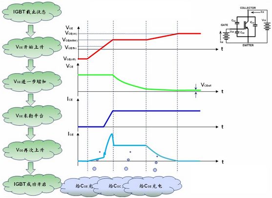
Picture 3. Diagram of IGBT activation process
Simulation of Drive Startup Process:
Picture 4. Analysis results of IGBT simulation model
b. Shutdown process
Time period t6:
This period is the shutdown delay time, and VGE decreases from VGG+to VGE with a time constant RG (Cge+Cgc, miller), while Io, VCE, and iC remain unchanged.
Time period t7:
VCE starts to rise, and the speed can be controlled by RG as follows:
Time period t8:
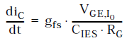
VCE remains at Vd, iC begins to decrease, and speed can also be controlled by RG, as follows:
Just like the moment of conduction, a peak voltage VLS=LS x diC/dt will be generated during the time periods of t7 and t8, superimposed on both ends of the IGBT collector emitter. This is the first of the two descending stages of iC, which is the process of partial disappearance of MOSFET current.
Time period t9:
The process in which the BJT part of the IGBT current iC disappears is often referred to as the trailing current. It is the current formed by the recombination behavior of minority carriers (holes) injected into the N-drift region. Therefore, the switching characteristics of IGBT are inferior to those of power MOSFETs.
The performance that IGBT drivers need to meet:
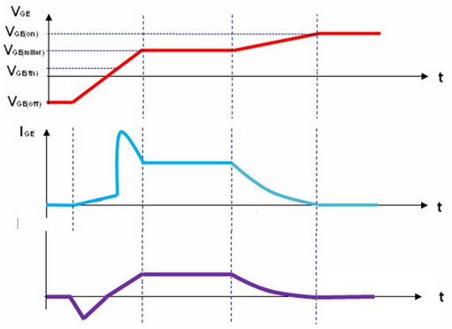
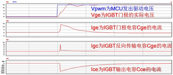
Picture 5. IGBT driving voltage and current waveform
1. To effectively drive IGBT, the energy supply of the driver must at least meet the driving loss requirements of IGBT;
2. When driving IGBT, there will be a significant current spike in the driving current, and the driver must have the ability to meet the requirements of the current spike during startup;
From the current mainstream IGBT driver products, the basic protection functions that IGBT drivers should have are mainly:
1. Undervoltage function, including primary input voltage undervoltage and secondary (i.e. IGBT terminal) undervoltage function;
2. Short circuit protection, also known as de saturation detection and protection;
3. Active clamping and Miller clamping protection;
These three are the main protective functions. Their respective focus areas are different.
Why do IGBT drivers need to design these cumbersome protection functions? This is determined by the characteristics of IGBT itself. IGBT can be seen as adding a thyristor on top of the MOSFET chip. The main purpose is to utilize the characteristics of MOSFETs that are easy to drive and turn off, as well as the durable nature of thyristors. It is undeniable that IGBT has indeed inherited these advantages.
From an equivalent model perspective, it can be seen that the input is MOSFET and the output is PNP transistor. However, due to the complexity of IGBT chips compared to MOSFETs, the consequence is that the parasitic parameters of IGBT are large. Moreover, due to the application of IGBT in high voltage and high current situations, the problem arises when too fast di/dt or dv/dt is combined with the large parasitic parameters of IGBT itself.
Therefore, efforts must be made on the IGBT driver. The IGBT driver itself is composed of circuits, which can introduce interference and parasitic parameters, especially in the case of high-frequency common mode interference, which can cause IGBT damage. The design of IGBT drivers is a challenge. The principle is not difficult. The difficulty lies in how to handle the effects of reducing parasitic parameters and common mode interference.